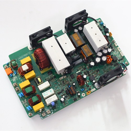
PCBA DIP processing
PCBA DIP processing refers to the processing flow of Dual In-line Package, which is an important part of the PCBA assembly process, especially for those large or special components that cannot be installed by surface mount technology (SMT).
PCBA DIP processing refers to the processing flow of Dual In-line Package, which is an important part of the PCBA assembly process, especially for large or special components that cannot be installed by surface mount technology (SMT).
The process flow of DIP processing usually includes the following steps:
1. Component pre-processing: Receive materials according to the BOM material list and perform pre-production pre-processing, such as foot cutting and molding. .
2. Plug-in: Manually insert the pre-processed components into the corresponding positions of the PCB board to prepare for the subsequent wave soldering.
3. Wave soldering: The plug-in PCB board passes through the wave soldering conveyor belt, and goes through the steps of spraying flux, preheating, wave soldering, cooling, etc. to complete the soldering.
4. Component foot cutting: Cut the feet of the soldered PCBA board to achieve the appropriate size.
5. Repair (post-welding): Repair and repair the PCBA finished boards that have been found to be incompletely welded.
6. Board cleaning: Remove the residual flux and other harmful substances on the PCBA finished products to achieve the cleanliness standard of environmental protection.
7. Functional test: Perform functional test on the welded PCBA finished boards to ensure that all functions are normal, and repair and retest the problems found.
- Previous:PCBA DIP plug-in processing
- Next:没有了


