1. Solder paste printing
Steps: Use a steel mesh to print the solder paste evenly onto the PCB pad.
Note: The steel mesh thickness, scraper pressure and angle must be precisely controlled to prevent
insufficient tin or bridging.
2. Component placement
Steps: Use a high-speed placement machine to accurately place SMD components on the PCB.
Note: Ensure accurate programming and unblocked nozzles to avoid offset or dropout.
3. Reflow soldering
Steps: The PCB enters the reflow oven and completes soldering according to the temperature curve.
Note: Control the preheating, reflow, and cooling curves to avoid cold soldering, cold soldering, or
overheating to damage components.
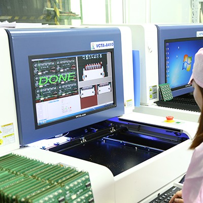
4. AOI inspection
Steps: Automatic optical inspection to check soldering quality.
Note: Focus on checking defects such as insufficient tin, short circuits, and tombstones to improve
the pass rate.
5. Manual soldering and repair
Steps: DIP plug-in soldering or rework abnormal solder joints.
Note: The temperature is moderate to prevent damage to the PCB or components.
6. Testing and Inspection
Steps: ICT, FCT and other tests to ensure that electrical performance meets the standards.
Note: The test fixture must be designed to match the design to ensure accurate testing.
7. Cleaning and Packaging
Steps: Remove residual flux and pack with anti-static treatment.
Note: Moisture-proof and anti-static to ensure safe transportation.


