- Home
- PCB
-
PCBA
- High-density PCBA (with BGA)
- RF PCBA
- Industrial control equipment PCBA
- Inverter energy storage PCBA
- Frequency conversion equipment PCBA
- Medical care PCBA
- Automotive electronics PCBA
- Digital product PCBA
- Internet of things PCBA
- Speaker audio PCBA
- Instrumentation PCBA
- LED lamp driver PCBA
- PCBA SMT patch processing
- PCBA DIP plug-in processing
- Industrial control box assembly and processing
- Application
- Support
- Factory
- News
- About


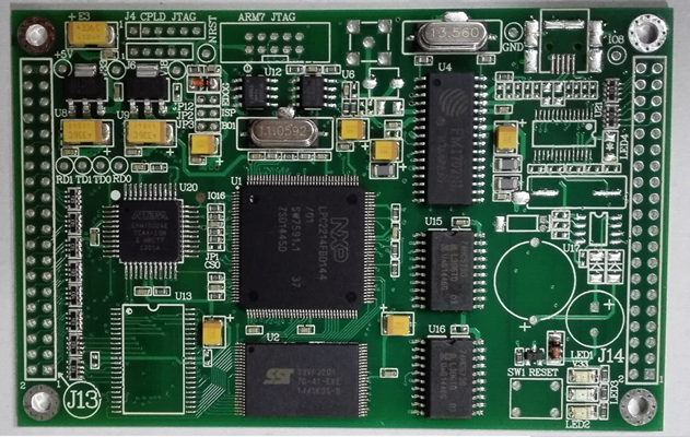
Medical imaging equipment PCB
Product Name: High TG PCB
Base Material: FR4, Aluminum
Copper Thickness: 0.5-4OZ / 1 Oz / 2Oz or Customized
Board Thickness: 0.2~6mm
Aperture: 0.15mm
Line Width: 0.015mm
Line Spacing: 0.015mm
Reliability of PCB for medical imaging equipment The design and manufacture of PCBs must meet strict medical standards and regulatory requirements, such as IPC-610, to ensure product reliability and durability.
With the development of technology With the development of medical imaging PCB, medical imaging PCB is constantly undergoing technological innovation and intelligent design. For example, high-density interconnect (HDI) PCB is increasingly used in medical imaging equipment, which provides higher data transmission speed and smaller The size helps to make the device smaller and more portable.
In addition, with the development of artificial intelligence technology With the development of AI medical imaging, the AI medical imaging market is growing rapidly and is expected to surge 10 times in the next decade to reach a market size of US$20 billion. The application of AI technology will further improve the diagnostic efficiency and accuracy of medical imaging equipment.
In terms of material selection, medical imaging PCB Special materials such as polytetrafluoroethylene (PTFE) and ceramic filler materials are often used, which have excellent electrical insulation properties and high-frequency characteristics, suitable for high-speed and high-frequency applications.
In short, medical Imaging PCB is the core component of medical imaging equipment. Its design and manufacturing need to consider signal integrity, electromagnetic compatibility (EMC), power consumption, reliability and intelligence to meet the medical industry's requirements for high performance and high reliability. With the continuous advancement of technology, medical imaging PCBs will continue to develop in the direction of higher performance, smaller size and intelligence.
- Previous:High TG PCB
- Next:Game console motherboard PCB
+008613530931324
Telephone: +008613530931324
Mail: Gelant.lei@kilandu.com
5th Floor, Building 4, Yibaolai Industrial City, Qiaotou Community, Fuhai Street, Bao'an District, Shenzhen
All rights reserved © 2024 Shenzhen Jintianlei Innovation Technology Co., Ltd.


