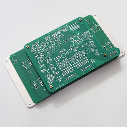
RF PCB
Product Category: RF RF PCB
Number of layers: 4 layers
Plate thickness: 1.6+/-0.25mm
< ;span style="font-family: arial, helvetica, sans-serif;">Size: 225.00mm*112.00mm
Minimum aperture: 0.3mm
< p style="text-align: left; text-indent: 0em;">Line width and line spacing: 0.1mm /0.1mmSurface treatment: FR-4
Product features: minimum hole copper thickness 25um, surface copper thickness 1oz
RF PCB is a printed circuit board used for the design and manufacture of radio frequency circuits, which specializes in processing radio frequency signals. Radio frequency signals generally refer to the frequency range in the electromagnetic spectrum used for wireless communications.
I. Features of RF PCB:
1. High-frequency materials: Materials such as polyimide (PI), polytetrafluoroethylene (PTFE, also known as Teflon) and aluminum nitride ceramics are used, which have low dielectric constants and loss factors at high frequencies.
2. Conductive materials: High-quality copper foil is used to make conductive wires to ensure smooth signal transmission.
3. Design complexity: Signal integrity needs to be considered to minimize signal crosstalk, ground plane splitting and noise coupling to enhance electromagnetic compatibility.
II. Application fields of RF PCB, including but not limited to:
1. Wireless communication: such as wireless network equipment, smart phones, smart TVs, etc.
2. Automotive electronics: used for communication systems inside cars.
3. Medical equipment: to achieve precise measurement, detection and monitoring functions.
4. Aerospace: Maintain stable communication performance in complex electromagnetic environments.
5. High-frequency applications: such as 5G base stations, satellite communications, etc., which require extremely high signal transmission quality.
- Previous:没有了
- Next:Electronic router RF PCB
