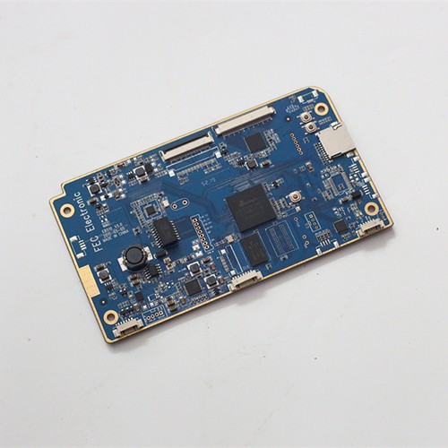
PCBA DIP plug-in processing
DIP (Dual In-line Package) in PCBA (Printed Circuit Board Assembly) is a common packaging method for electronic components.
Preparation work: including preparing the materials and tools required for circuit boards, components, sockets, etc.
BOM verification and process arrangement: verify the material model and specifications according to the BOM (bill of materials), arrange the process, and assign components to each work station.
Plug-in: insert the DIP packaged components into the corresponding sockets of the circuit board according to the circuit design requirements.
Soldering: electrically connect the pins of the components to the pads on the circuit board through wave soldering, manual soldering and other welding methods.
Inspection and testing: inspect the soldered circuit board to ensure that the components are correctly installed and there are no problems such as cold soldering and short circuit, and then perform functional testing to verify whether the performance of the circuit board meets the design requirements.
Maintenance and debugging: If problems are found during the inspection or testing process, the circuit board needs to be repaired or debugged to ensure product quality.
Cleaning and drying: Clean the soldered circuit board to remove the flux and other residues on the surface, and then dry it for subsequent processes.
- Previous:没有了
- Next:PCBA DIP processing


